Home /
Expert Answers /
Computer Science /
vhdl-code-up-down-counter-implementation-on-7-segment-display-tablel-clarify-the-operation-type-whic-pa115
(Solved): vhdl code Up/down counter implementation on 7-Segment display Tablel clarify the operation type whic ...
vhdl code
Up/down counter implementation on 7-Segment display
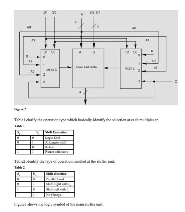
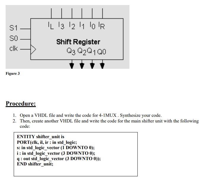
Tablel clarify the operation type which basically identify the selection at each multiplexer. Table 1 Table2 identify the type of operation handled at the shifter unit. Table 2 Figure3 shows the logic symbol of the main shifter unit.
Figure 3 Procedure: 1. Open a VHDL file and write the code for 4-1MUX. Synthesize your code. 2. Then, create another VHDL file and write the code for the main shifter unit with the following code: ENTITY shifter_unit is PORT(clk, il, ir : in std_logic; s: in std_logic_vector(1 DOWNTO 0); : in std_logic_vector (3 DOWNTO 0); q : out std_logic_vector (3 DOWNTO 0)); END shifter_unit;
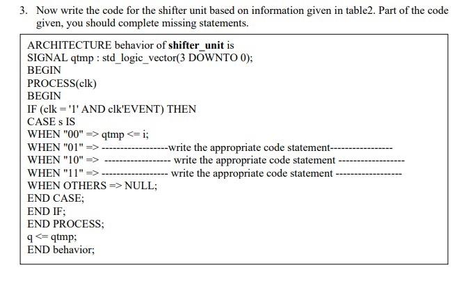
3. Now write the code for the shifter unit based on information given in table2. Part of the code given, you should complete missing statements.
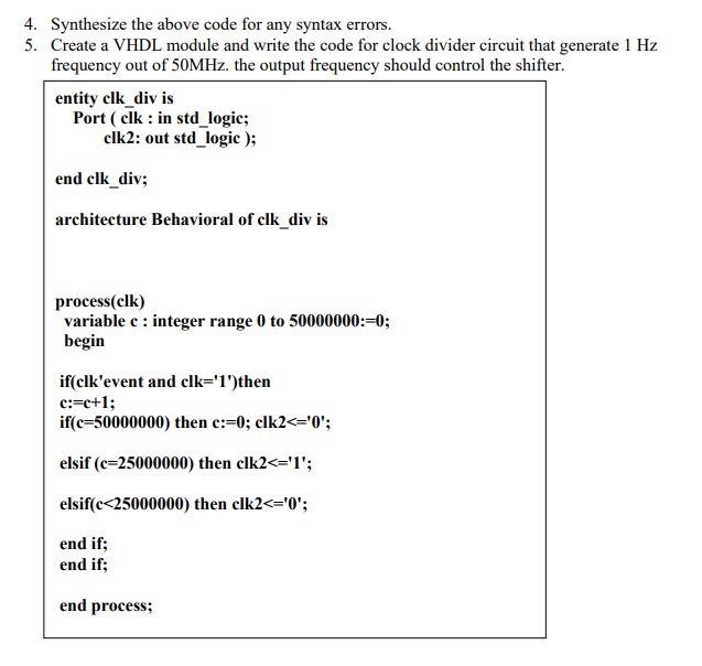
4. Synthesize the above code for any syntax errors. 5. Create a VHDL module and write the code for clock divider circuit that generate frequency out of . the output frequency should control the shifter. entity clk_div is Port (clk : in std logic; clk2: out std_logic); end clk_div; architecture Behavioral of clk_div is process(clk) variable c : integer range 0 to ; begin if(clk'event and clk='1') then if then clk ; elsif then clk ; elsif then clk ; end if; end if; end process;
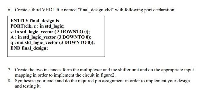
6. Create a third VHDL file named "final_design.vhd" with following port declaration: ENTITY final_design is PORT(clk, c : in std logic; s: in std_logic_vector DOWNTO 0; A : in std_logic_vector DOWNTO 0; q : out std_logic_vector (3 DOWNTO 0)); END final_design; 7. Create the two instances form the multiplexer and the shifter unit and do the appropriate input mapping in order to implement the circuit in figure2. 8. Synthesize your code and do the required pin assignment in order to implement your design and testing it.
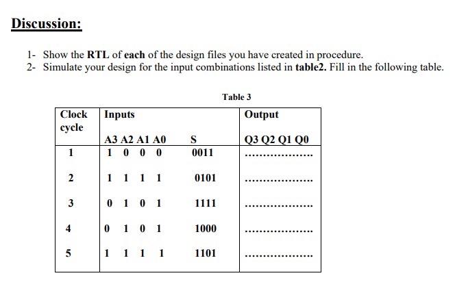
1- Show the RTL of each of the design files you have created in procedure. 2- Simulate your design for the input combinations listed in table2. Fill in the following table.