Home /
Expert Answers /
Electrical Engineering /
question-1-the-band-structure-of-indium-phosphide-mathrm-inp-and-silicon-si-a-pa831
(Solved): Question \( 1 . \) The band structure of indium phosphide ( \( \mathrm{InP}) \) and silicon (Si) a ...
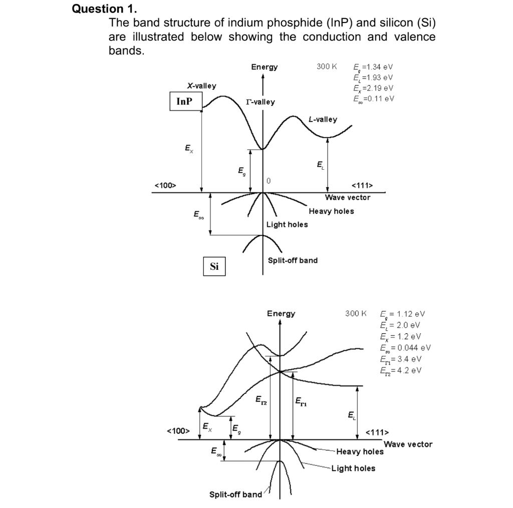
Question \( 1 . \) The band structure of indium phosphide ( \( \mathrm{InP}) \) and silicon (Si) are illustrated below showing the conduction and valence bands.
(a) Using the illustrations, identify the band gap type and associated band gap energy for both materials. Explain what material would be an efficient light emitter and why. [4 marks] (b) Calculate the wavelengths above which the two materials become transparent. [4 marks] (c) Draw the energy band diagram and the Fermi energy for intrinsic silicon. Calculate the resistance of a cube of length \( 1 \mathrm{~cm} \) of intrinsic silicon at a temperature of \( 300 \mathrm{~K} \). The electron and hole mobilities are: \( \mu_{n}=1500 \mathrm{~cm}^{2} \cdot V^{-1} \cdot \mathrm{s}^{-1} \) and \( \mu_{p}=458 \mathrm{~cm}^{2} \cdot V^{-1} \cdot \mathrm{s}^{-1} \) [6 marks] (d) Draw the energy band diagram and the Fermi energy for silicon with and without an applied electric field in the two following cases: - Doped with a phosphorus concentration on the order of \( 1 \times 10^{18} \mathrm{~cm}^{-3} \) - Doped with a boron concentration on the order of \( 1 \times 10^{18} \) \( \mathrm{cm}^{-3} \) [6 marks]
Question \( 2 . \) A silicon wafer has a pn-junction where the acceptor impurity concentration \( \left(N_{A}\right) \) is \( 2 \times 10^{17} \mathrm{~cm}^{-3} \) and the donor concentration \( \left(N_{D}\right) \) is \( 1 \times 10^{17} \mathrm{~cm}^{-3} \). (a) Sketch band diagrams showing the pn-junction at equilibrium, under a forward bias and under a reverse bias. Illustrate the most important carrier flows in each diagram. [10 marks] (b) The \( \mathrm{P} \) type of the wafer is now doped to a level \( \left(N_{A}\right) \) of \( 4 \times 10^{17} \mathrm{~cm}^{-3} \), the donor concentration \( \left(N_{D}\right) \) remains at \( 1 \times 10^{17} \) \( \mathrm{cm}^{-3} \). i. Calculate the built-in potential \( \emptyset_{b i} \). ii. Calculate the depletion width \( W \). iii. Comment on the location of the depletion layer in the pnjunction. [10 marks]
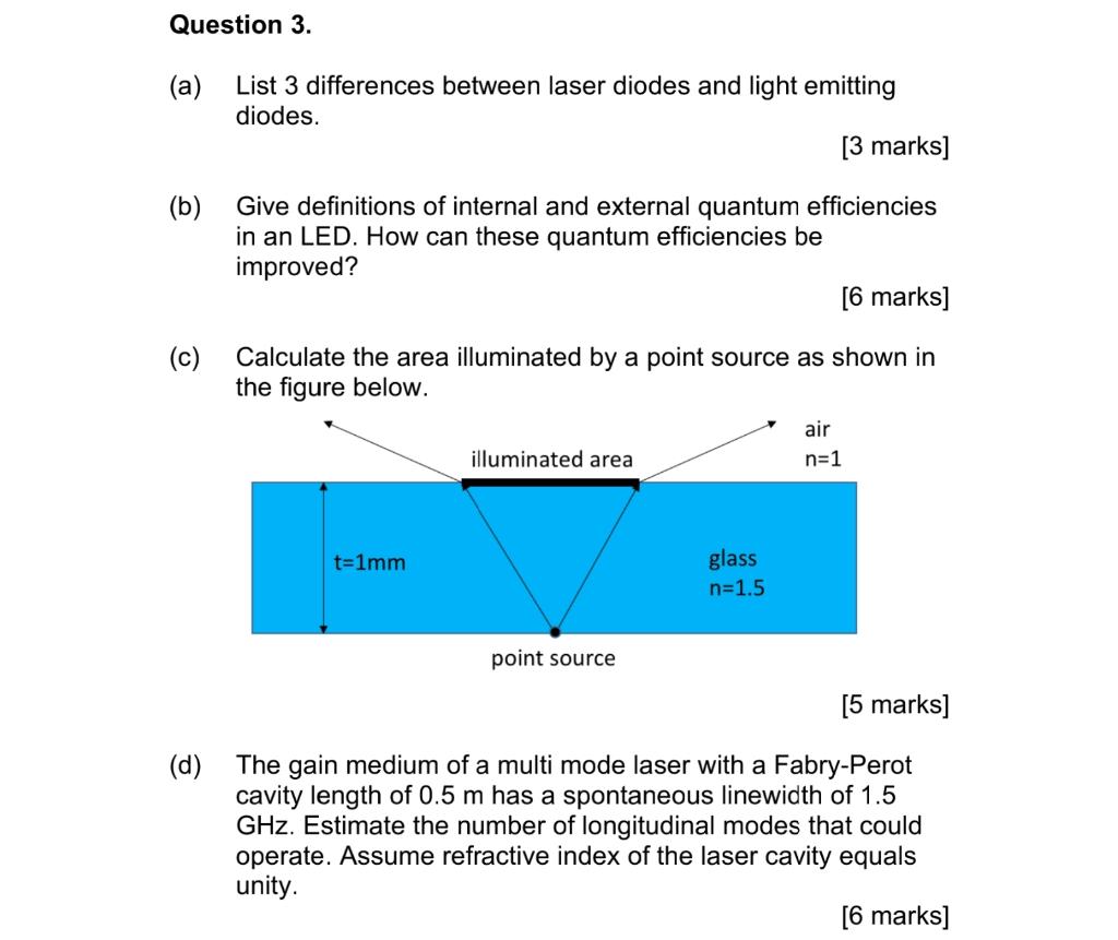
Give definitions of internal and external quantum efficiencies in an LED. How can these quantum efficiencies be improved? [6 marks] c) Calculate the area illuminated by a point source as shown in the figure below. [5 marks] d) The gain medium of a multi mode laser with a Fabry-Perot cavity length of \( 0.5 \mathrm{~m} \) has a spontaneous linewidth of \( 1.5 \) \( \mathrm{GHz} \). Estimate the number of longitudinal modes that could operate. Assume refractive index of the laser cavity equals unity. [6 marks]
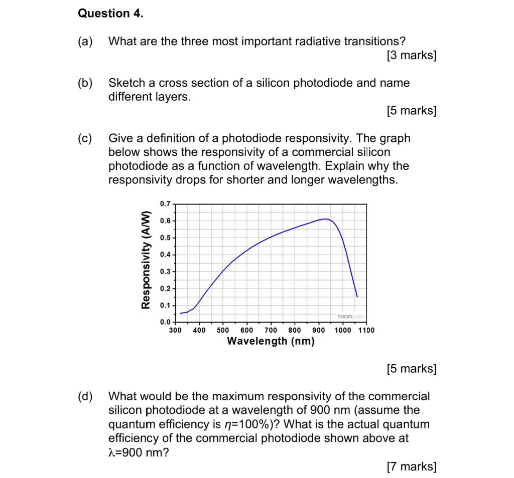
Give a definition of a photodiode responsivity. The graph below shows the responsivity of a commercial silicon photodiode as a function of wavelength. Explain why the responsivity drops for shorter and longer wavelengths. [5 marks] 4) What would be the maximum responsivity of the commercial silicon photodiode at a wavelength of \( 900 \mathrm{~nm} \) (assume the quantum efficiency is \( \eta=100 \%) \) ? What is the actual quantum efficiency of the commercial photodiode shown above at \( \lambda=900 \mathrm{~nm} \) ? [7 marks]
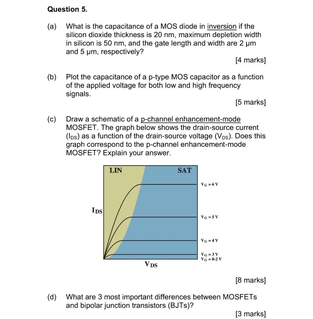
(b) Plot the capacitance of a p-type MOS capacitor as a function of the applied voltage for both low and high frequency signals. \( [5 \) marks \( ] \) (c) Draw a schematic of a p-channel enhancement-mode MOSFET. The graph below shows the drain-source current \( \left(I_{D S}\right) \) as a function of the drain-source voltage \( \left(V_{D S}\right) \). Does this graph correspond to the p-channel enhancement-mode MOSFET? Explain your answer. [8 marks] (d) What are 3 most important differences between MOSFETs and bipolar junction transistors (BJTs)? [3 marks]
Expert Answer
question 2 i.diference betweem LED and Laser: LED STANDS FOR LIGHT-EMITTING DIODE It is multicoloured. It is incoherent. It is caused by spontaneous emission. It is not directional. Low energy is related LEDs are small in size, have a long life, are