Home /
Expert Answers /
Computer Science /
part1-procedure-follow-all-instructions-below-a-a-logic-diagram-for-the-full-adder-is-shown-pa844
(Solved): PART1: Procedure: Follow all instructions below. a) A logic diagram for the full adder is shown ...
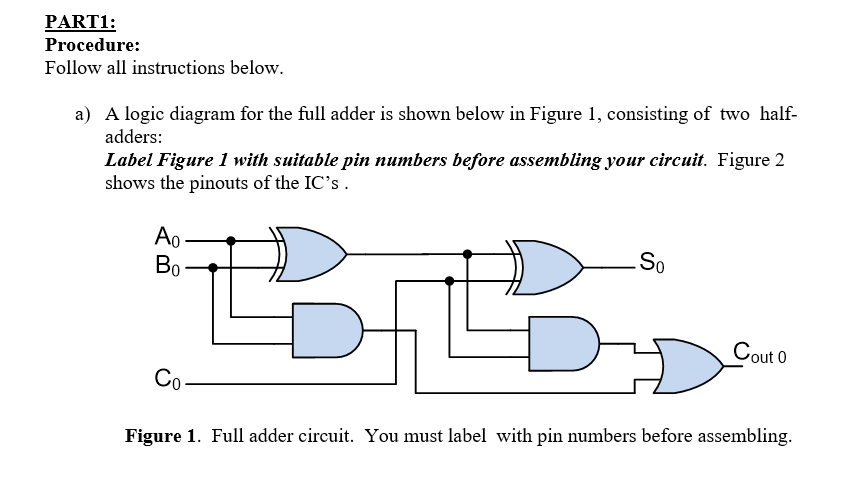
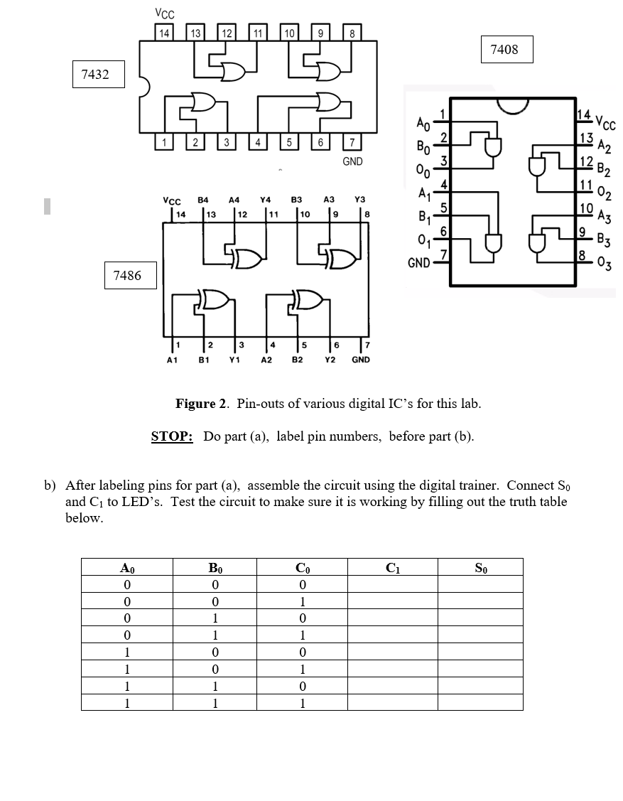
PART1: Procedure: Follow all instructions below. a) A logic diagram for the full adder is shown below in Figure 1, consisting of two halfadders: Label Figure 1 with suitable pin numbers before assembling your circuit. Figure 2 shows the pinouts of the IC's. Figure 1. Full adder circuit. You must label with pin numbers before assembling.
Figure 2. Pin-outs of various digital IC's for this lab. STOP: Do part (a), label pin numbers, before part (b). b) After labeling pins for part (a), assemble the circuit using the digital trainer. Connect and to LED's. Test the circuit to make sure it is working by filling out the truth table below.
Expert Answer
a)............................?ans: The logic Diagram and output of the full adder (consisting of 2 half adders and 1 OR gate) are: from Figure 1