Home /
Expert Answers /
Electrical Engineering /
experiment-2-bjt-as-an-amplifier-a-bjt-can-be-configured-in-three-ways-depending-on-which-terminal-pa226
(Solved): Experiment 2: BJT as an Amplifier A BJT can be configured in three ways depending on which terminal ...
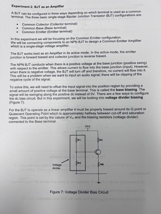
Experiment 2: BJT as an Amplifier A BJT can be configured in three ways depending on which terminal is used as a common terminal. The three basic single-stage Bipolar Junction Transistor (BJT) configurations are: - Common Collector (Collector terminal) - Common Base (Base terminal) - Common Emitter (Emitter terminal) In this experiment we will be focusing on the Common Emitter configuration. We will be connecting components to an NPN BJT to design a Common Emitter Amplifier which is a single-stage voltage amplifier. The BJT works best as an Amplifier in its active mode. In the active mode, the emitter junction is forward biased and collector junction is reverse biased. The NPN B.JT conducts when there is a positive voltage at the base junction (positive swing) with respect to the emitter. This allows current to flow into the base junction (input). However, when there is negative voltage, the BJT will turn off and therefore, no current will flow into it. This will be a problem when we want to input an audio signal; there will be clipping of the negative cycle of the signal. To solve this, we will need to offset the input signal into the position region by providing a small amount of positive voltage at the base terminal. This is called the base biasing. The signal will be swinging along the positive dc instead of . There are a few ways to configure the dc bias circuit. But in this experiment, we will be looking into voltage divider biasing (Figure 7). For the BJT to operate as a linear amplifier it must be properly biased around its Q point or Quiescent Operating Point which is approximately halfway between cut-off and saturation region. This point is set by the values of and the biasing resistors (voltage divider) connected to the Base terminal. Figure 7: Voltage Divider Bias Circuit
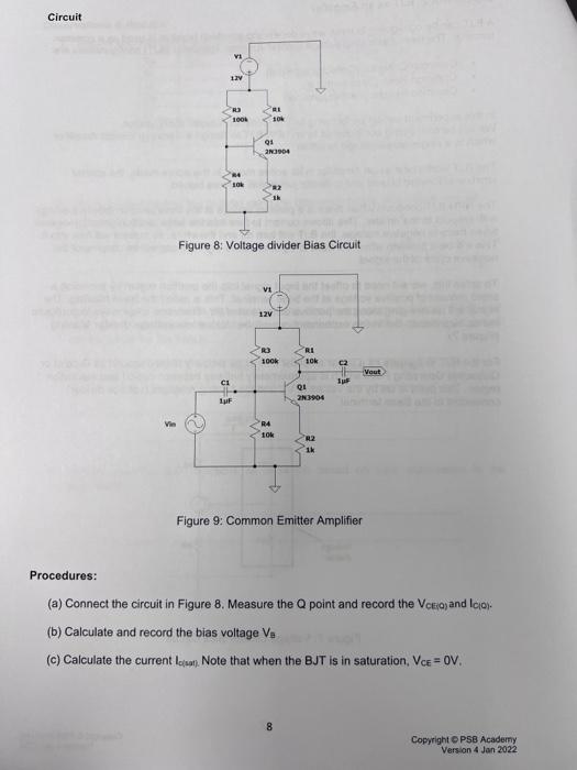
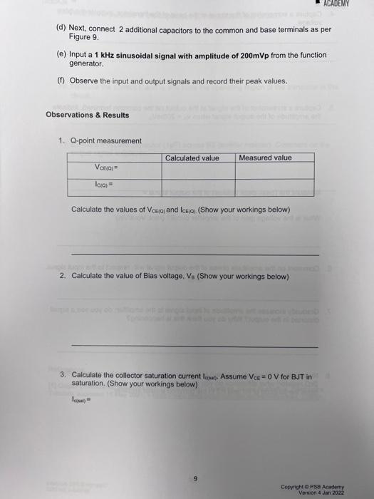
Figure 8 : voltage divider blas circuit Figure 9: Common Emitter Amplifier Procedures: (a) Connect the circuit in Figure 8. Measure the Q point and record the V(ceio) and lcior. (b) Calculate and record the bias voltage (c) Calculate the current Losati. Note that when the BJT is in saturation, .
(d) Next, connect 2 additional capacitors to the common and base terminals as per Figure 9. (e) Input a sinusoidal signal with amplitude of from the function generator. (f) Observe the input and output signals and record their peak values. Observations \& Results 1. Q-point measurement Calculate the values of and lceiol. (Show your workings below) 2. Calculate the value of Bias voltage, (Show your workings below) 3. Calculate the collector saturation current . Assume for BJT in saturation. (Show your workings below)
4. Capture a screenshot of the signal at the base of the transistor. Indicate the bias voltage. 5. Capture a screenshot of the signal at the output (at the common terminal). Indicate the amplitude of the output signal when . Measure the (peak-peak voltage) of the output signal = What is the voltage gain of the amplifier circuit? (Hint: Vout/in) 6. Comment on the amplitude phase of the output signal with respect to the input signal. 7. Gradually increase the amplitude of input signal to the amplifier; do you see a signal distorted in the output? Why do you think this is happening? 8. Reduce the R1 (collector resistor) to a lower value : ( For example replaced with a resistor) what difference do you see in the output? State the function of R1 and R2 in the common emitter amplifier.
9. What is the purpose of the capacitors ( and ) in this circuit? 10. Measure the current and and state the operating region of the transistor in the circuit. 11. Connect a bypass capacitor across (emitter resistor). Comment on the output signal amplitude. END References: [1] Output Characteristics Curves of a Typical Bipolar Transistor, Digital Illustration, Electronics Tutorials, accessed 11 May 2021, ?