Home /
Expert Answers /
Advanced Physics /
consider-the-nfet-layout-shown-in-figure-4-begin-array-l-w-6-mu-mat-pa944
(Solved): Consider the nFET layout shown in Figure 4 . \[ \begin{array}{l} W=6 \mu \mat ...
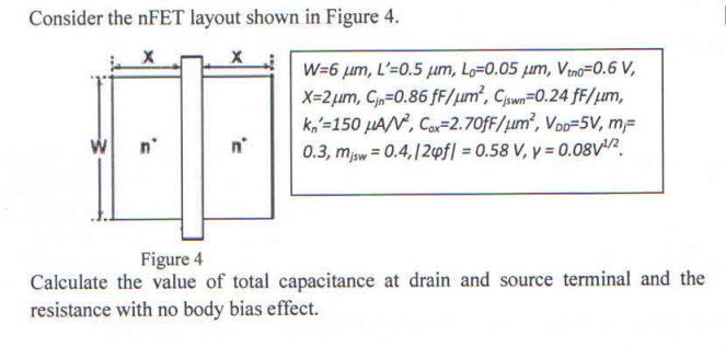
Consider the nFET layout shown in Figure 4 . \[ \begin{array}{l} W=6 \mu \mathrm{m}, L^{\prime}=0.5 \mu \mathrm{m}, L_{0}=0.05 \mu \mathrm{m}, V_{\mathrm{tn} 0}=0.6 \mathrm{~V}, \\ X=2 \mu \mathrm{m}, C_{j n}=0.86 \mathrm{fF} / \mu \mathrm{m}^{2}, C_{j \mathrm{swn}}=0.24 \mathrm{fF} / \mu \mathrm{m}, \\ k_{n}^{\prime}=150 \mu \mathrm{A} / \mathrm{V}^{2}, C_{o x}=2.70 \mathrm{fF} / \mu \mathrm{m}^{2}, V_{D D}=5 \mathrm{~V}, m_{j}= \\ 0.3, m_{j \mathrm{sw}}=0.4, \mid 2 \varphi f /=0.58 \mathrm{~V}, y=0.08 \mathrm{~V}^{1 / 2} . \end{array} \] Figure 4 Calculate the value of total capacitance at drain and source terminal and the resistance with no body bias effect.
Expert Answer
To calculate the total capacitance at the drain and source terminals, we need to consider the following three types of capacitance: Capacitance betwee