Home /
Expert Answers /
Chemical Engineering /
28-6-a-horizontal-chemical-vapor-deposition-cvd-reactor-similar-to-the-configuration-shown-in-exa-pa993
(Solved): 28.6 A horizontal chemical vapor deposition (CVD) reactor similar to the configuration shown in Exa ...
28.6 A horizontal chemical vapor deposition (CVD) reactor similar to the configuration shown in Example 3, Figure 28.6 will be used for growth of gallium arsenide (GaAs) thin films. In this process, arsine vapor, trimethylgallium vapor, and gas are fed into the reactor. Inside the reactor, the silicon wafer rests on a heated plate called a susceptor. The reactant gases flow parallel to the surface of the wafer and deposit a GaAs thin film according to the simplified CVD reactions If the reactant gas is considerably diluted in gas, then the mass transfer of each species in the carrier gas can be treated separately. These surface reactions are considered to be very rapid, and so the mass transfer of the gaseous reactants to the surface of the wafer limits the rate of GaAs thin-film formation. In the present process, a square silicon wafer is positioned at the leading edge of the susceptor plate. The process temperature is , and the total system pressure (1.0 atm). The feed gas delivered to the reactor results in a bulk linear velocity of . The composition of arsine and trimethylgallium in the feed gas are both 0.10 mole\%, which is very dilute. You may assume that the amount of arsine and trimethylgallium delivered with the feed gas is much higher than the amount of arsine and trimethylgallium consumed by the reactions, so that the concentration of these reactants in the bulk gas phase is essentially constant down the length of the reactor. You may also assume that the surface-reaction rates are instantaneous relative to the rates of mass transfer, so that the gasphase concentrations of both arsine vapor and trimethylgallium vapor at the surface of the wafer are essentially zero. The binary gas-phase diffusion coefficient of trimethylgallium in is 1.55 at and . a. What are the average mass-transfer rates for arsine and trimethylgallium over the whole wafer? b. Based on the ratio of the arsine and trimethylgallium masstransfer rates, what is the composition of the GaAs composite thin film-e.g., the molar composition of gallium and arsenic (As) in the solid? How could the feed-gas composition be adjusted so that the molar ratio of Ga to As within the solid thin film is ?
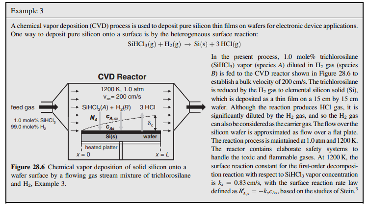
A chemical vapor deposition (CVD) process is used to deposit pure silicon thin films on wafers for electronic device applications. One way to deposit pure silicon onto a surface is by the heterogeneous surface reaction: In the present process, 1.0 mole\% trichlorosilane ( ) vapor (species ) diluted in gas (species ) is fed to the CVD reactor shown in Figure 28.6 to establish a bulk velocity of . The trichlorosilane is reduced by the gas to elemental silicon solid (Si), which is deposited as a thin film on a by wafer. Although the reaction produces gas, it is significantly diluted by the gas, and so the gas can also be considered as the carrier gas. The flow over the silicon wafer is approximated as flow over a flat plate. The reaction process is maintained at and . The reactor contains elaborate safety systems to handle the toxic and flammable gases. At , the Figure 28.6 Chemical vapor deposition of solid silicon onto a wafer surface by a flowing gas stream mixture of trichlorosilane and , Example 3 . surface reaction constant for the first-order decomposition reaction with respect to vapor concentration is , with the surface reaction rate law defined as , based on the studies of Stein.
Expert Answer
a. To calculate the average mass-transfer rates for arsine (AsH3) and trimethylgallium (Ga(CH3)3) over the whole wafer, we need to consider the diffusion of each species in the H2 carrier gas. The mass-transfer rate is given by Fick's Law: Mass-transfer rate = D * A * (C_surface - C_bulk) / L Where: D is the diffusion coefficient, A is the area of the wafer, C_surface is the concentration at the surface of the wafer (assumed to be zero), C_bulk is the bulk concentration, and L is the thickness of the wafer.