Home /
Expert Answers /
Electrical Engineering /
2-a-based-on-the-circuit-shown-in-fig-q2a-i-plot-v-x-vs-v-text-in-and-pa271
(Solved): 2. a) Based on the circuit shown in Fig. Q2a, (i) plot \( V_{X} \) vs \( V_{\text {in }} \) and \( ...
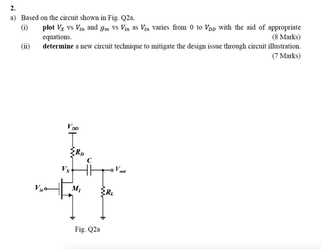
2. a) Based on the circuit shown in Fig. Q2a, (i) plot \( V_{X} \) vs \( V_{\text {in }} \) and \( g_{m} \) vs \( V_{i n} \) as \( V_{\text {in }} \) varies from 0 to \( V_{D D} \) with the aid of appropriate equations. (8 Marks) (ii) determine a new circuit technique to mitigate the design issue through circuit illustration. (7 Marks)