Home /
Expert Answers /
Electrical Engineering /
18-1-recall-that-mos-transistors-are-symmetrical-and-that-what-distinguishes-the-source-from-the-dra-pa466
(Solved): 18.1 Recall that MOS transistors are symmetrical and that what distinguishes the source from the dra ...
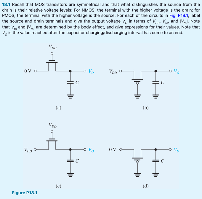
18.1 Recall that MOS transistors are symmetrical and that what distinguishes the source from the
drain is their relative voltage levels: For NMOS, the terminal with the higher voltage is the drain; for
PMOS, the terminal with the higher voltage is the source. For each of the circuits in Fig. P18.1, label
the source and drain terminals and give the output voltage V_(o) in terms of V_(DD^('))V_(tn^(')) and |V_(tp)|. Note
that V_(tn) and |V_(tp)| are determined by the body effect, and give expressions for their values. Note that
V_(0) is the value reached after the capacitor chargin(g)/(d)ischarging interval has come to an end.
(a)
(d)
Figure P18.1