Home /
Expert Answers /
Electrical Engineering /
1-analysis-and-design-of-a-buck-boost-converter-a-buck-boost-converter-is-illustrated-below-pa645
(Solved): 1. Analysis and design of a buck-boost converter. A buck-boost converter is illustrated below. ...
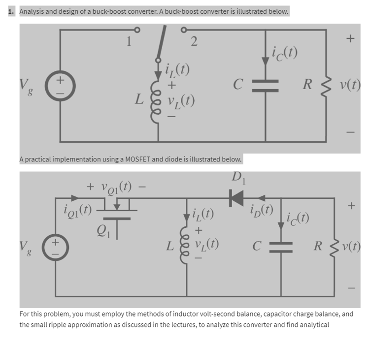
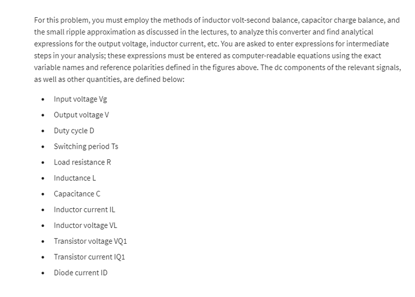

1. Analysis and design of a buck-boost converter. A buck-boost converter is illustrated below. V 8 V. + 8 1 A practical implementation using a MOSFET and diode is illustrated below. D? + Voi(t) — T ign(t) ‚i(t) + v?(t) - 2 L i?(t) + V? (1) ic(t) in(t) ? R ic(t) R + v(t) + v(t) For this problem, you must employ the methods of inductor volt-second balance, capacitor charge balance, and the small ripple approximation as discussed in the lectures, to analyze this converter and find analytical
For this problem, you must employ the methods of inductor volt-second balance, capacitor charge balance, and the small ripple approximation as discussed in the lectures, to analyze this converter and find analytical expressions for the output voltage, inductor current, etc. You are asked to enter expressions for intermediate steps in your analysis; these expressions must be entered as computer-readable equations using the exact variable names and reference polarities defined in the figures above. The dc components of the relevant signals, as well as other quantities, are defined below: ? . Input voltage Vg Output voltage V Duty cycle D Switching period Ts Load resistance R Inductance L Capacitance C Inductor current IL Inductor voltage VL Transistor voltage VQ1 Transistor current IQ1 Diode current ID
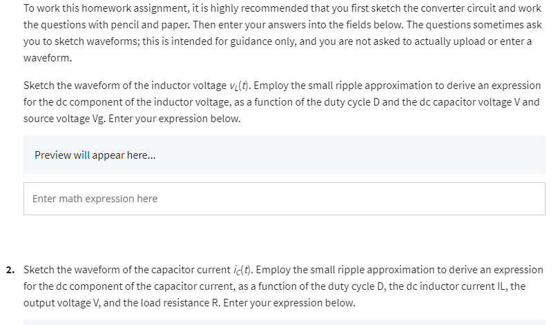
To work this homework assignment, it is highly recommended that you first sketch the converter circuit and work the questions with pencil and paper. Then enter your answers into the fields below. The questions sometimes ask you to sketch waveforms; this is intended for guidance only, and you are not asked to actually upload or enter a waveform. Sketch the waveform of the inductor voltage v?(t). Employ the small ripple approximation to derive an expression for the dc component of the inductor voltage, as a function of the duty cycle D and the dc capacitor voltage V and source voltage Vg. Enter your expression below. Preview will appear here... Enter math expression here 2. Sketch the waveform of the capacitor current ic(t). Employ the small ripple approximation to derive an expression for the dc component of the capacitor current, as a function of the duty cycle D, the dc inductor current IL, the output voltage V, and the load resistance R. Enter your expression below.
6. Derive an expression for the capacitor peak voltage ripple (denoted "delta v" in the lectures). Express your result in terms of Vg, D, Ts, C, and R, and enter the result below. Assume that the capacitor is ideal and lossless. Preview will appear here... Enter math expression here 1 point
Expert Answer
Answer:- asper chegg guidel